Direct laser writing (DLW) via multiphoton absorption has been widely used for creating three-dimensional, complex features in materials such as glass and polymer. In the context of polymer-dispersed liquid crystals (LCs), DLW based on two-photon absorption has been employed to control the interplay between the refractive indices of the polymer network and the LC components.

Wiley
Now, Chloe Tartan and colleagues from the UK and Slovenia have further demonstrated the use of aberration-corrected DLW to create read-on-demand micrometre-scale patterns in polymerizable LC devices (Adv. Opt. Mater. https://doi.org/10.1002/adom.201800515; 2018). Their approach is unique in that polymer microstructures are generated directly within a switchable LC device, and that under specific voltage conditions the refractive indices of the polymer and LC can be matched, making the polymer microstructures invisible.
In their work, a polymerizable LC mixture, comprising ~70 wt% nematic LC host and ~30 wt% of a reactive mesogen and photoinitiator mixture, is capillary-filled in the isotropic liquid phase into a LC cell. The cell consists of two parallel glass plates that are coated with the transparent conductive oxide, indium tin oxide, and a rubbed polyimide alignment layer. The LC device is mounted onto the translation stage stack in the DLW system and connected to a waveform generator so that an electric field can be applied to the device during fabrication.
When femtosecond laser pulses of 100 fs duration at 790 nm with a repetition rate of 80 MHz are incident on the LC device via a 0.3 NA objective lens, two-photon absorption by the photoinitiator triggers crosslinking of the reactive mesogen, creating a pillar structure of a dense polymer network that locks-in the voltage-dependent LC director profile at the moment of exposure to the laser beam. Adaptive optics is used to correct for the optical aberrations that are introduced by the air/glass interface so that micrometre-sized features can be written directly into the LC device. The laser-written polymer pillars have dimensions of 1 μm in diameter and 5 μm in height.
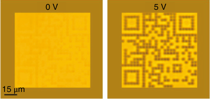
The nonlinear nature of the two-photon polymerization process, which takes place during exposure to the DLW, ensures that the precise alignment of the LC molecules is only ‘frozen-in’ around a small region defined by the laser focus. Different LC alignments can be frozen-in to the pillars by electrically switching the LC device to different voltage amplitudes during the DLW process. By using the same voltage amplitude that is used to write the polymer structures to read the devices, features can be made to disappear as the LC director profile becomes homogeneous with the surrounding regions. This way the features can be cloaked for both polarized and unpolarized light. When the electric field is removed, the polymer features are clearly distinguishable from the surrounding LC region so that patterns can be observed.
By tailoring the write and read voltages, the researchers have shown that it is possible to make polymer pillars appear and disappear in the LC host. It is also possible to reconfigure the structures so that different features or patterns emerge at different voltage amplitudes. The team applied the technique to create micrometre-scale features, such as reconfigurable bicycle symbols, emoticons and quick-response codes (pictured).
“The advantage of this approach is that by combining direct laser writing with aberration correction, we can write into fully assembled liquid-crystal devices, allowing us to create a wide range of structures and architectures at the micrometre scale, and potentially even at nanometre-scale resolution,” said Stephen Morris from the University of Oxford, UK to Nature Photonics. When asked about their future work, he added “we are currently exploring the smallest feature size that can be achieved using this technique. The limitation is likely to be down to the diffusion of the polymer network during the polymerization process, and this is something that we are currently investigating.”
The researchers see the potential of this technique being in the areas of security, anti-counterfeiting and product authentication. “For example, display manufacturers would be able to encode their displays with a ‘watermark’ feature that would only become readable under specific voltage configurations and sequences,” said Morris.