Attosecond science after the prize: instruments, not products
Pulses short enough to resolve electron motion won the 2023 physics Nobel. The applications remain firmly in fundamental research, and that is worth stating plainly.
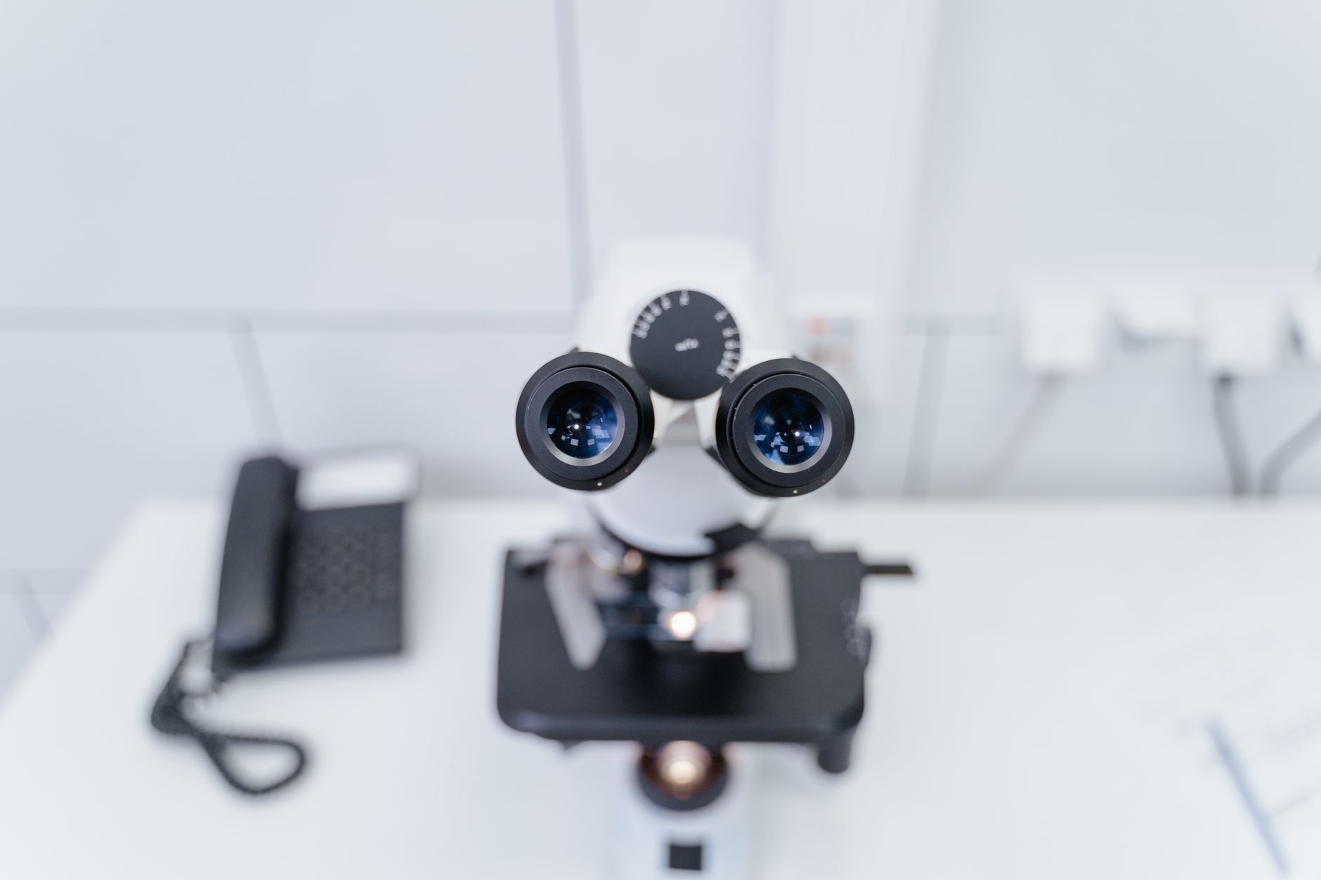
The 2023 Nobel Prize in Physics recognised methods generating attosecond pulses of light. An attosecond is 10⁻¹⁸ seconds; the timescale matters because electron motion in atoms and molecules occurs there. Femtosecond pulses resolve nuclear motion; attosecond pulses reach the electrons.
How the pulses are made
The dominant route is high harmonic generation. An intense femtosecond pulse is focused into a gas. The field pulls an electron from an atom, accelerates it, and drives it back as the field reverses. The recollision emits a burst of high-frequency light, in the extreme ultraviolet or soft X-ray, lasting attoseconds.
The process is inefficient — conversion is very low — and the output is at wavelengths that most optics absorb, so beamlines operate in vacuum with grazing-incidence or multilayer optics.
What it is used for
Charge migration. Watching charge redistribute across a molecule after ionisation, on its natural timescale, which has implications for photochemistry and for understanding radiation damage.
Photoemission timing. Measuring the delay between photon absorption and electron emission, a quantity that turned out not to be zero and that constrains theory.
Solid-state dynamics. Following carrier motion in semiconductors and dielectrics on timescales relevant to how fast electronics could in principle switch.
Why applications stay fundamental
The measurements require a vacuum beamline, sophisticated detection and considerable expertise. Signal levels are low, acquisition is slow, and samples must suit the geometry.
None of that resembles an industrial measurement. Suggestions that attosecond methods will find near-term application in semiconductor metrology or materials characterisation are speculative, and the field's own practitioners are generally careful about it.
What does transfer
The enabling technologies spread outward. High-power femtosecond drivers developed for attosecond generation are the same class of source used in industrial micromachining. Extreme ultraviolet optics developed for these beamlines share problems with EUV lithography. Detection and timing techniques propagate into other measurement fields.
That is the realistic account of the field's industrial relevance: it is a demanding customer whose requirements pull component technology forward, rather than a source of processes that factories will adopt.
This article was produced by the LasersNews AI desk and reviewed by our editors.
Related reading
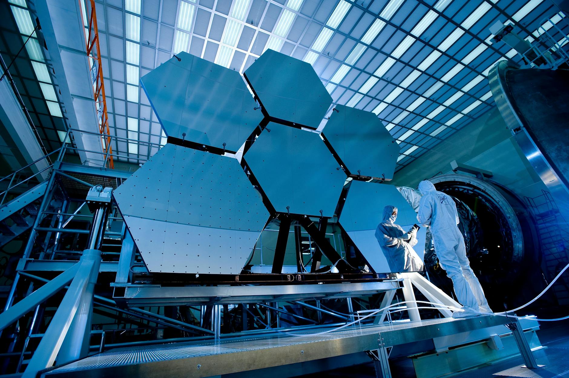
Integrated photonics narrows the gap between laboratory result and manufacturable part
Foundry access and standardised process design kits are doing for photonics roughly what they did for electro…
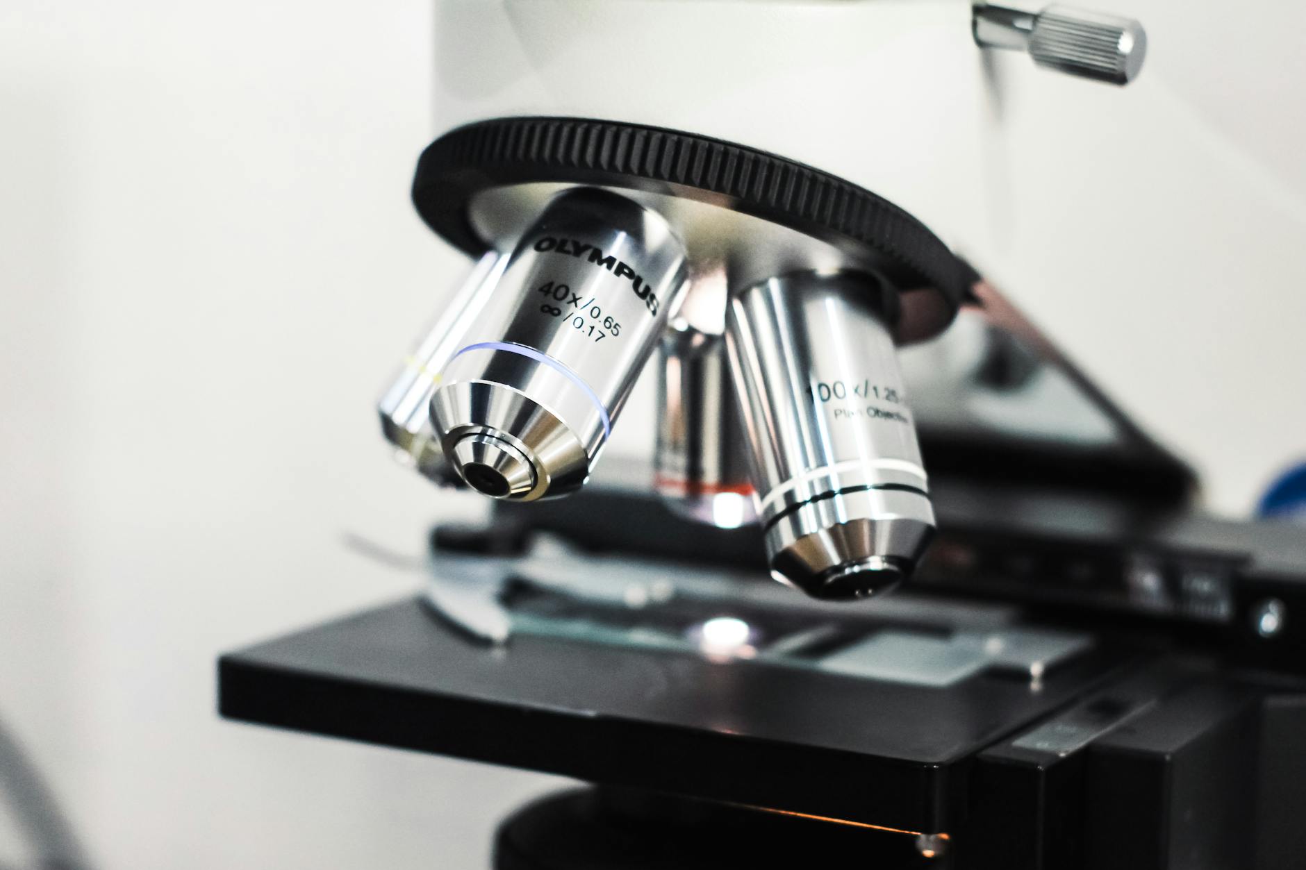
Metasurface optics are running into the manufacturing question
Flat lenses built from sub-wavelength structures work. Producing them at volume, at yield, with the tolerance…
Photonics found its foundry model, and the effect resembles electronics in the 1980s
Shared process design kits and multi-project wafer runs let a small team design a photonic chip without ownin…